

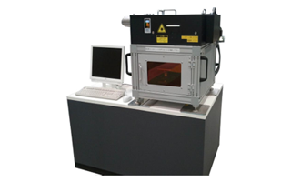
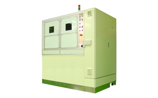
Our Laser Machining Division supply 266nm deep-UV laser machining systems, laser markers, and laser scribers based on unique wavelength conversion technology. The use of this wavelength enables nearly HAZ(heat-affected-zone)-free micromachining on different types of raw materials—metals, resins, composite materials, and semiconductor materials. We also accept orders for small-quantity prototyping and small-quantity contract processing.

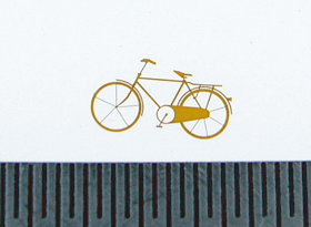
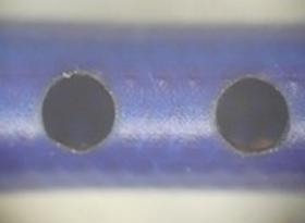
Capable of machining various materials
- Efficient laser power absorption into different materials.
- Low in residuals from the photolytic processing of resins and compound semiconductors.
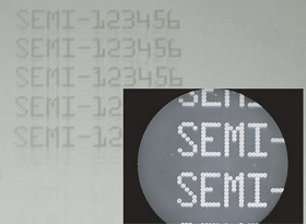
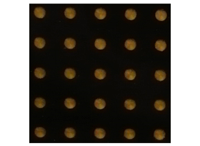
Capable of micromachining
- Micromachining with a machining spot diameter of 15 to 20 μm
(variable depending on the material).
Capable of photolytic processing
- Sharp surface processing low in residuals.
Processing with high flexibility
- Combination of a high-precision galvano scanner and an orthogonal two-axial stage for
for high-speed, high-precision maskless processing.
- Preinstalled software for easy processing pattern programming.
Easy operation
- Only needs power, no gases required.
- Air-cooled, no coolant required.
Because of its nature, a laser beam is capable of increasingly minute machining in inverse proportion to the wavelength. Conversely, a short wavelength laser is extremely difficult to handle, and practical use in FA(factory automation) applications has been difficult because of reliability, stability, and the service life of the wavelength conversion crystal. The Division promoted research and development of wavelength conversion technology, parts, and unit products for the stable generation of short-wavelength fourth-harmonic wave (266nm) and successfully developed a laser oscillator with a stable, long service life. The technology has enabled micromachining, micromarking, and microscribing on different metals, resins, composite materials, and semiconducting materials and has come into use in different industrial scenes.
![]()
![]()